2 Layer LED PCB
- PRODUCT DETAIL
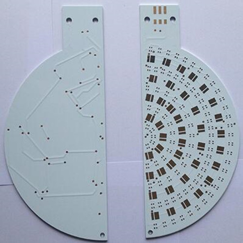
2 Layer LED PCB
1.The specific description about LED PCB as following ,pls see:
1.The specific description about LED PCB as following ,pls see:
Base Material: FR4
Layer:2
Board Thickness:1.6mm+/-10%
Finished Copper:1oz
Solder Mask:super white
Silkscreen: black color
Surface finishing:HASL-Lead Free
Outline Profile: CNC routing/Punching
All pcb of the parameters can be customized!
2.Purchase Tips:
If you want to purchase 2 Layer LED PCB, please provide a formal PCB Gerber files and your detailed requirement to us.
Thanks for your contacting RayMing LED PCB in advance,we are your trustworthy LED PCB Supplier for any heart of your successful business.
3.Delivery Timescales
A:Sample:
Single layer 3~5days
Double Side 4-6days
Urgent sample prototype could be pushed 2-3 days earlier with premium.
B:Mass Production:
Single layer standard 5~8days
Double Side standard 7~10days
For more depends your specific quantity.
4.Package & Shipping Method:
1. Inner vacuum package for pcb board,and filled with foam, Outer carton box with packing belt.
2. By DHL, UPS, FedEx, TNT
3. By EMS (Usually for Russia Clients)
4. By sea for mass quantity according to customer's requirement.
5.Payment method
1. T/T
2. Paypal
3. Western Union
6.Primary Competitive Advantages:
Country of Origin
Green Product
Price
Product Performance
Quality Approvals
Service
Small Orders Accepted
Experience
2 Layer LED PCB
1.The specific description about LED PCB as following ,pls see:
1.The specific description about LED PCB as following ,pls see:
Base Material: FR4
Layer:2
Board Thickness:1.6mm+/-10%
Finished Copper:1oz
Solder Mask:super white
Silkscreen: black color
Surface finishing:HASL-Lead Free
Outline Profile: CNC routing/Punching
All pcb of the parameters can be customized!
2.Purchase Tips:
If you want to purchase 2 Layer LED PCB, please provide a formal PCB Gerber files and your detailed requirement to us.
Thanks for your contacting RayMing LED PCB in advance,we are your trustworthy LED PCB Supplier for any heart of your successful business.
3.Delivery Timescales
A:Sample:
Single layer 3~5days
Double Side 4-6days
Urgent sample prototype could be pushed 2-3 days earlier with premium.
B:Mass Production:
Single layer standard 5~8days
Double Side standard 7~10days
For more depends your specific quantity.
4.Package & Shipping Method:
1. Inner vacuum package for pcb board,and filled with foam, Outer carton box with packing belt.
2. By DHL, UPS, FedEx, TNT
3. By EMS (Usually for Russia Clients)
4. By sea for mass quantity according to customer's requirement.
5.Payment method
1. T/T
2. Paypal
3. Western Union
6.Primary Competitive Advantages:
Country of Origin
Green Product
Price
Product Performance
Quality Approvals
Service
Small Orders Accepted


